 high performance
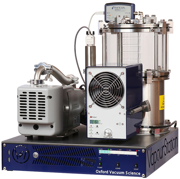 bench-top thin film from
Thin film deposition is a process in which the physical characteristics of a surface are modified by applying a very thin coating, often just a few millionths of a millimetre thick. Thin films can be used to modify the optical characteristics of a surface (the substrate), its electrical conductivity, its hardness or lubricity, to provide corrosion resistance or chemical inertness, or simply for decoration. Every-day examples of thin films include the reflective coating on CDs and DVDs, anti-reflective coatings on spectalces and thermally efficient double glazing (optical films), the tiny electrical pathways within a micro-processor (electrical films), hardened machine tool bits (hardness), to food and drug packaging (decoration and passivation).
In order to produce such thin films, the deposit must be applied in a very controlled manner, sometimes even atomic monolayer by atomic monolayer, under extremely clean, particulate free conditions. Individual depositing particles must be able to travel from some deposition source to the substrate to be coated with little or no collision with gas molecules on the way (a long 'mean free path') - thin film deposition is a high vacuum process.
Thin film deposition processes broadly fall into two catagories:- chemical vapour deposition (CVD) and physical vapour deposition (PVD). In CVD the substrate is exposed to one or more volatile precursors, which react and/or decompose on the substrate surface to produce the desired deposit. Frequently, volatile by-products are also produced, which are removed by gas flow through the reaction chamber. The growth of the film is often enhanced either by heating the substrate, or by using a plasma to increase the density of reactive species (free radicals). In some cases both are used, such as in the deposition of diamond like carbon (DLC) where carbon is deposited at high temperatures (typically in excess of 800°C) from a methane precursor in a dense Hydrogen plasma.
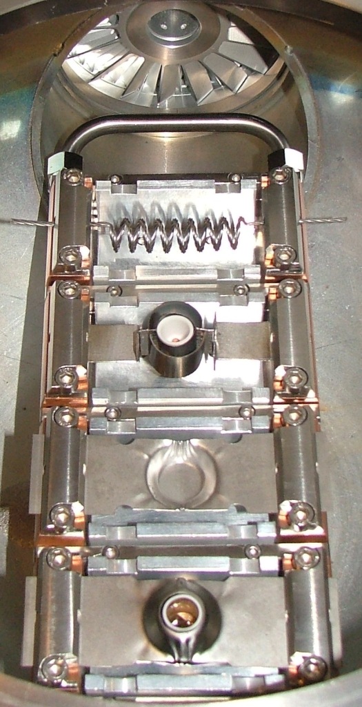
PVD uses mechanical or thermodynamic means to produce the thin film. The principal mechanical method is a technique known as sputtering, where energetic noble gas ions, most commonly Argon, bombard the surface of a target made from the desired film material, releasing a plume of material from the target - like the shower of earth produced when a shell hits the ground - which then embeds itself into the surface of the substrate. Thermal evaporation (thermodynamic means) is a process in which a solid piece of the desired film material is heated until it melts and then evaporates or until it sublimes. Under high vacuum the vapour follows a direct line of sight path to the substrate where it condenses to form the thin film.
In general metals are easier to deposit than dielectrics with PVD, so a common technique is to sputter or evaporate from a metal source but in the presence of a partial pressure (perhaps 10-2mbar) of a reactive gas. For example, Aluminium might be evaporated in the presence of Oxygen to deposit Alumina. As with CVD, heat and/or plasma is often used to enhance film growth, particularly in reactive processes.
Oxford Vacuum Science manufactures bench-top thin film deposition systems for research and light industrial applications. For more details contact technology@oxford-vacuum.com or click on the contact link.
Oxford Vacuum Science Ltd
18 Enstone Road
Middle Barton
Oxfordshire
OX7 7BN UK
tel: +44 (0) 7495 463875
OVS@oxford-vacuum.com